- 您现在的位置:买卖IC网 > Sheet目录356 > SI8220BD-A-IS (Silicon Laboratories Inc)IC ISODRIVER 2.5A OPTO IN 16SOIC
Si8220/21
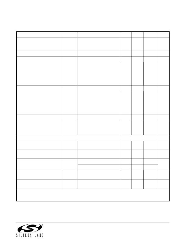
Table 1. Electrical Characteristics (Continued) 1
V DD = 12 V or 15 V, V SS = GND, T A = –40 to +125 °C; typical specs at 25 °C.
Parameter
Symbol
Test Conditions
Min
Typ
Max
Units
I R = 10 mA.
Input Reverse Voltage
BV R
Measured at ANODE with
0.5
—
—
V
respect to CATHODE.
Input Capacitance
C IN
—
10
—
pF
VDD Undervoltage Threshold 2
VDD UV+
V DD rising
5 V Threshold
8 V Threshold
10 V Threshold
12.5 V Threshold
See Figure 9 on page 15.
See Figure 10 on page 15.
See Figure 11 on page 15.
See Figure 12 on page 15.
5.20
7.50
9.60
12.4
5.80
8.60
11.1
13.8
6.30
9.40
12.2
14.8
V
V
V
VDD Undervoltage Threshold 2
VDD UV–
V DD falling
5 V Threshold
8 V Threshold
10 V Threshold
12.5 V Threshold
See Figure 9 on page 15.
See Figure 10 on page 15.
See Figure 11 on page 15.
See Figure 12 on page 15.
4.90
7.20
9.40
11.6
5.52
8.10
10.1
12.8
6.0
8.70
10.9
13.8
V
V
V
VDD Lockout Hysteresis
VDD Lockout Hysteresis
VDD Lockout Hysteresis
VDD HYS
VDD HYS
VDD HYS
UVLO voltage = 5 V
UVLO voltage = 8 V
UVLO voltage = 10 V or
12.5 V
—
—
—
280
600
1000
—
—
—
mV
mV
mV
AC Specifications
Propagation Delay Time to High
Output Level
Propagation Delay Time to Low
Output Level
Output Rise and Fall Time
Device Startup Time
Common Mode
Transient Immunity
t PLH
t PHL
t R , t F
t START
CMTI
C L = 200 pF
C L = 200 pF
(0.5 A), C L = 200 pF
(2.5 A), C L = 200 pF
Time from
V DD = V DD_UV+ to V O
Input ON or OFF
V CM = 1500 V (see Figure 3)
—
—
—
—
—
—
—
—
—
—
—
30
60
40
30
20
40
—
ns
ns
ns
μs
kV/μs
Notes:
1. VDD = 12 V for 5, 8, and 10 V UVLO devices; VDD = 15 V for 12.5 V UVLO devices.
2. See "9.Ordering Guide" on page 22 for more information.
Rev. 1.4
5
发布紧急采购,3分钟左右您将得到回复。
相关PDF资料
SI8402AB-B-IS
IC I2C ISOLATOR BIDIR 8-SOIC
SI8405AB-A-IS1
IC ISOLATOR 10M 6CH 2.5K 16SOIC
SI8423BD-B-IS
ISOLATOR 2CH 5KV 150M 16SOIC
SI8435BB-C-IS1
IC ISOLATOR DGTL 3CH 16SOIC
SI8442BB-C-IS1
IC ISOLATOR DGTL 4CH 16SOIC
SI8451BB-A-IS1
IC ISOLATOR DGTL 5CH 16SOIC
SI8460BB-A-IS1
IC ISOLATOR DGTL 6CH 16SOIC
SI8606AC-B-IS1
IC ISOLATOR BIDIR 3.75KV 16SOIC
相关代理商/技术参数
SI8220BD-A-ISR
功能描述:IC ISODRIVER 2.5A OPTO IN 16SOIC RoHS:是 类别:隔离器 >> 数字隔离器 系列:- 产品培训模块:IsoLoop® Isolator 标准包装:50 系列:IsoLoop® 输入 - 1 侧/2 侧:5/0 通道数:5 电源电压:3 V ~ 5.5 V 电压 - 隔离:2500Vrms 数据速率:110Mbps 传输延迟:12ns 输出类型:CMOS 封装/外壳:16-SOIC(0.154",3.90mm 宽) 供应商设备封装:16-SOIC N 包装:管件 工作温度:-40°C ~ 85°C 其它名称:390-1053-5
Si8220-B-IP
功能描述:隔离器接口集成电路 2.5A Single ISOdriver w/Opto In RoHS:否 制造商:Texas Instruments 通道数量:2 传播延迟时间: 电源电压-最大:5.5 V 电源电压-最小:3 V 电源电流:3.6 mA 功率耗散: 最大工作温度:+ 125 C 安装风格: 封装 / 箱体:SOIC-8 封装:Tube
Si8220CB-A-IS
功能描述:隔离器接口集成电路 2.5kV 2.5A Opto Input ISOdriver RoHS:否 制造商:Texas Instruments 通道数量:2 传播延迟时间: 电源电压-最大:5.5 V 电源电压-最小:3 V 电源电流:3.6 mA 功率耗散: 最大工作温度:+ 125 C 安装风格: 封装 / 箱体:SOIC-8 封装:Tube
SI8220CB-A-ISR
功能描述:IC ISODRIVER 2.5A OPTO INP 8SOIC RoHS:是 类别:隔离器 >> 数字隔离器 系列:- 产品培训模块:IsoLoop® Isolator 标准包装:50 系列:IsoLoop® 输入 - 1 侧/2 侧:5/0 通道数:5 电源电压:3 V ~ 5.5 V 电压 - 隔离:2500Vrms 数据速率:110Mbps 传输延迟:12ns 输出类型:CMOS 封装/外壳:16-SOIC(0.154",3.90mm 宽) 供应商设备封装:16-SOIC N 包装:管件 工作温度:-40°C ~ 85°C 其它名称:390-1053-5
Si8220CB-D-IS
制造商:Silicon Laboratories Inc 功能描述:2.5kV 2.5A Opto Input ISOdriver
Si8220CD-A-IS
功能描述:隔离器接口集成电路 5.0kV 2.5A Opto Input ISOdriver RoHS:否 制造商:Texas Instruments 通道数量:2 传播延迟时间: 电源电压-最大:5.5 V 电源电压-最小:3 V 电源电流:3.6 mA 功率耗散: 最大工作温度:+ 125 C 安装风格: 封装 / 箱体:SOIC-8 封装:Tube
SI8220CD-A-ISR
功能描述:IC ISODRIVER 2.5A OPTO IN 16SOIC RoHS:是 类别:隔离器 >> 数字隔离器 系列:- 产品培训模块:IsoLoop® Isolator 标准包装:50 系列:IsoLoop® 输入 - 1 侧/2 侧:5/0 通道数:5 电源电压:3 V ~ 5.5 V 电压 - 隔离:2500Vrms 数据速率:110Mbps 传输延迟:12ns 输出类型:CMOS 封装/外壳:16-SOIC(0.154",3.90mm 宽) 供应商设备封装:16-SOIC N 包装:管件 工作温度:-40°C ~ 85°C 其它名称:390-1053-5
Si8220DB-A-IS
功能描述:隔离器接口集成电路 2.5kV 2.5A Opto Input ISOdriver RoHS:否 制造商:Texas Instruments 通道数量:2 传播延迟时间: 电源电压-最大:5.5 V 电源电压-最小:3 V 电源电流:3.6 mA 功率耗散: 最大工作温度:+ 125 C 安装风格: 封装 / 箱体:SOIC-8 封装:Tube
